FPGA development, HDL and digital logic verification
Design starts from frequencies, throughput, latency and available signals. The split between programmable logic and firmware considers parallelism, resources and testability. Simulation and implementation are compared so correct testbench behaviour does not conceal timing or reset problems.
Activities and verification
HDL modules, streaming interfaces and registers accessible from software.
Testbenches for normal sequences, limits, resets and clock-domain crossings.
Analyse timing constraints, resource use and tests on the board.
Initial decisions and integration
I clarify electrical and logical interfaces, clocks, resets, numerical precision and the existing synthesis flow. Work can cover an HDL block, verification or software integration, following the team’s conventions and review process.
A verification example
For an acquisition path, expected and produced data, resets and boundary conditions are compared. Functional simulation, clock-domain crossing analysis and static timing serve different purposes. A testbench does not replace CDC analysis or implementation timing constraints.
Deliverables and acceptance criteria
HDL sources, testbenches, constraints, synthesis instructions and verification results. Acceptance frequency, latency and throughput refer to the agreed FPGA and configuration.
Where to start
Provide the FPGA device, toolchain, signal specification and sample data to process.
Can you work on the logic without redesigning the board?
Yes, when hardware, access and documentation allow a focused engagement. Scope can cover only HDL, a testbench or the firmware interface.
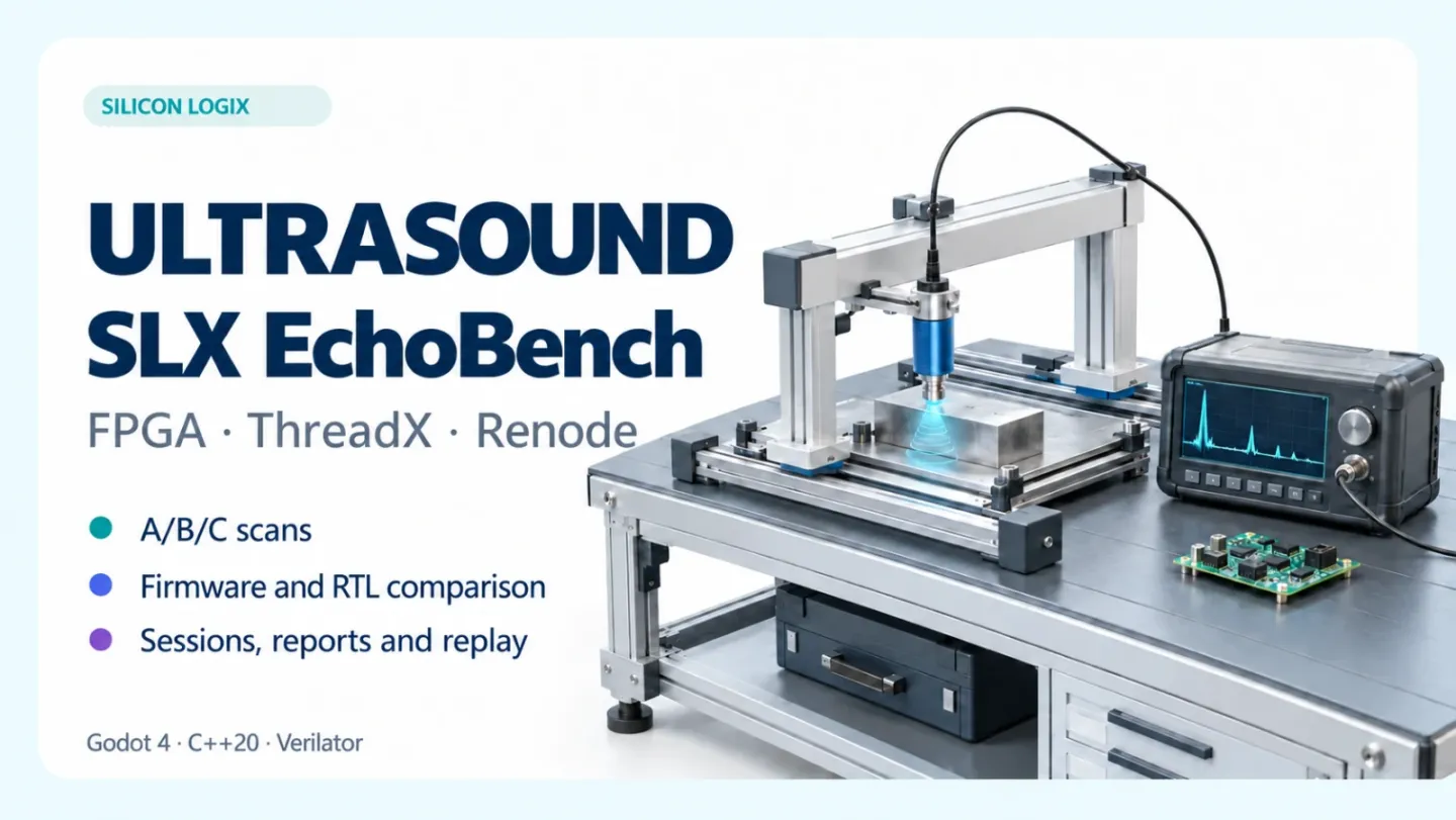
SLX EchoBench connects synthetic ultrasound, ThreadX firmware and RTL verification through Renode, Verilator, Godot and C++20. Explore the 3D bench, reproduce FIFO overflow and compare firmware on the same saved input. Windows preview on GitHub.